Eesti teaduse teekaardi objekt NAMUR+
Litography services
Institute of Physics at University of Tartu offers possibility to use photolithography and electron beam lithography services for fabrication of resist masks on planar substrates.
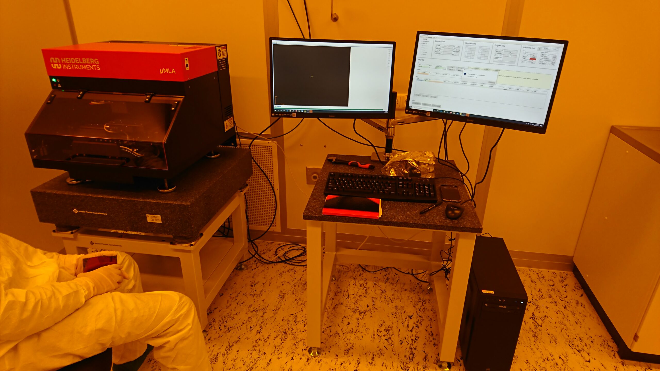
Photolithography enables making binary structures in photoresist onto substrates using UV light. The resultant structures in the photoresist can be used as masks for materials deposition (e.g. metal deposition) or etching (e.g. silicon etch) and can be subsequently conveniently removed using appropriate organic solvents, such as acetone. The photoresist itself can also act as a functional layer. Maskless aligner Heidelberg Instruments μMLA for photolithography exposes CAD designs straight on the samples without the need to fabricate a separate photomask. Patterns are exposed on substrates in raster scan mode with UV LED operating at 390 nm. Minimum structure size is under 1 µm and write speeds up to 100 mm2/min are possible, regardless of the complexity of the design. μMLA accommodates samples as small as 5 mm × 5 mm, and up to 5” × 5” (127 mm × 127 mm). Wide variety of positive and negative photoresists at different thicknesses can be used. In addition to binary structures, μMLA can also write 3D structures using grayscale lithography. The applications range from electrical contact manufacturing and microfluidics channels creation to complex surface pattern generation.

The lithography complex is located in an ISO 5 cleanroom with yellow light and is equipped with necessary substrate processing tools, e.g. spin coater, hot plates and wet bench. A precision manual diamond scriber (AVT Technologie GmbH RV-129) can be used to dice larger substrates.
Electron beam (e-beam) lithography uses electrons instead of photons to create the patterns in resist. The lithography complex has a Raith Elphy Quantum nanopatterning attachment coupled with a FEI Helios NanoLab 600 SEM, enabling e-beam lithography with minimum structure size <100 nm.
Services include:
- consultation – scientific and/or technical matters will be discussed with the client and evaluated, if chosen methods will meet the client interest;
- sample preparation, exposure, development and inspection done by a qualified and experienced lithography engineer;
- interpretation and analysis of the results (if needed);
- development activities that the given infrastructure allows for solving specific problems of the client, i.e. new research methods or specific sample processing can be developed and/or implemented;
- research – our specialists work closely with the client to solve their complex problems. Normally these are the situations where single analysis or measurement is not enough and the scientific-technical problem needs wider investigations.
There is possibility for training courses, related to the methods of micro and nano fabrication, for the technical staff of clients.

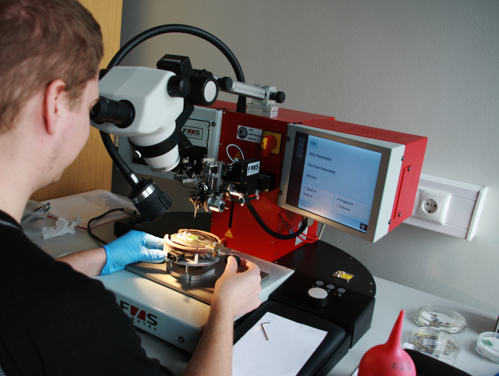
The wire bonder 53xxBDA (F&S Bondtec Semiconductor GmbH) is a part of lithography complex. The wire bonder enables preparation of electrical connections to microscopic electronic devices. The wire bonder allows ball bonding with gold wires with diameters ranging from 17.5 to 50 µm and wedge-wedge bonding with aluminium and gold wires with diameters ranging from 17.5 to 75 µm or with gold ribbons with sizes ranging from 30 × 12 µm to 250 × 25 µm.

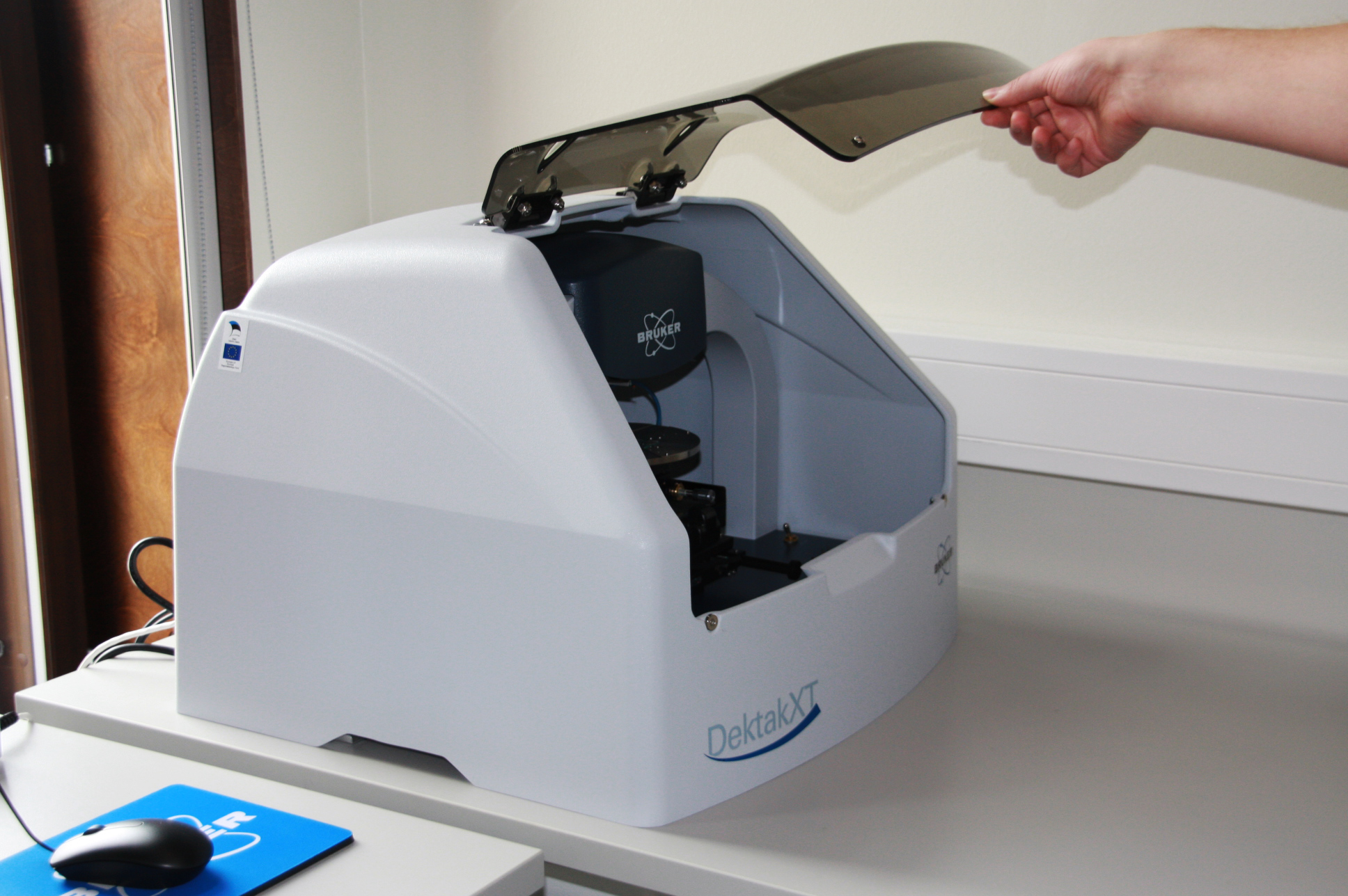
Part of lithography complex is also profilometer DektakXT Stylus Profiler for measurements of surface profiles, including to control litography processes.
Contact person: Kaupo Kukli (e-mail: kaupo.kukli@ut.ee)
Estonian Research Infrastructures Roadmap object „Center of nanomaterials technologies and research (NAMUR+)” is co-fundeded by European Regional Development Fund (projects „Nanomaterials – research and applications“, 3.2.0304.12-0397, 01.02.2012-31.12.2015 and „Center of nanomaterials technologies and research”, 2014-2020.4.01.16-0123, 01.01.2017-30.06.2022).


